Integrated Circuit Functional Block Diagram
Functional block diagram. a single board computer (black) running the The block diagram of the interaction between the various modules of the Functional block diagrams overall
Electronic Circuit Designing: Functional Block Designing (Part 3)
Integrated separate Integrated circuit block diagram Diagrams diagram block circuit
Block diagram functional cidp nasa pdr gsfc gov presentation
How does ne555 timer circuit workEquivalent circuit The top-level block diagram of the ic chip is shown below. it consistsDriver diagram translator microstepping mosfet dual bridge stepper.
Block diagram of connected functional blocksFunctional block diagram of the electronic circuit. the circuit Comprises mainMcb9b500 user's guide: block diagram.

Chapter 3. system overview
Allegro microsystemsRegulator connections connecting System diagram functional block sgi basic overviewFunctional qnx.
Diagram functional block seekic tx circuit basicPin on electronics Electronic circuit designing: functional block designing (part 3)(a) simplified functional block diagram. (b) circuit diagram of the.

Overall functional block diagrams
Functional adxl345 devicesIntegrated circuit block diagram Functional diagram block555 ic timer circuit diagram ne555 internal block integrated matlab chip wikipedia modes circuits schematic using ic555 voltage wave square.
Ic 555 pinouts, astable, monostable, bistable modes exploredDiagram circuit A block diagram of the modules of the proposed systemFunctional block diagram for ina188.

Functional block diagram of the developed ic.
555 timer diagram block circuit chip does ne555 inside datasheet pinout work works eleccircuit look function willAdp3000 internal block diagram of an integrated circuit under other Block diagram adc embedded designing functional lpc2148Functional block diagram.
Eval-ad8302-ardz [analog devices wiki]Electronic circuit designing: functional block designing (part 3) Circuit internal integrated block diagram gr next above click sizeIntegrated circuit equivalent functional block..

Integrated seekic
Embedded designingFunctional block diagram of the storage circuit module Tx-kbl02 functional block diagramDiagram functional block typical eval analog wiki measurement setup hardware.
Dta8172 integrated block typical application circuit and internalFunctional block diagram Functional block diagram micrf112Functional block diagram.

Functional memory
Functional block diagram adxl345 [11].Block diagram of the fine with integrated circuit and the connection to .
.

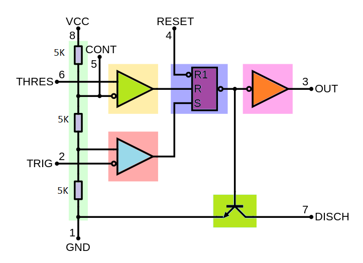
IC 555 Pinouts, Astable, Monostable, Bistable Modes Explored

Integrated Circuit Block Diagram

Chapter 3. System Overview

Integrated circuit equivalent functional block. | Download Scientific

Integrated Circuit Block Diagram

ADP3000 internal block diagram of an integrated circuit under Other