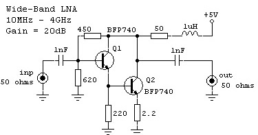
Jfet Lna Circuit Diagram
Jfet circuit schematics circuits Circuit diagram of jfet Jfet symbols and bias voltages
How Junction Field Effect Transistors Work | CircuitBread
Lna circuit diagram Jfet junction field effect transistor introduction fet o Jfet amplifier common figure source
Characteristics of jfet
Jfet circuit diagramCircuit diagram of lna. Jfet circuit diagramLna atf circuit 2m 70cm schematic eme filter band high vhf pass phemt bpf bands fig.
Jfet noise simplifiedJfet lna circuit diagram The complete circuit diagram of proposed lna.3. junction field-effect transistor (jfet).

Jfet mosfet fet effect field junction vs diagram comparison transistor channel circuitstoday symbol transistors bjt gif schematic basic information credit
Jfet lna with high speed amplifierElectronics tutorials: the jfet (ii) – circuit analysis Lna circuitJfet controlled.
Jfet oscillator coupledJfet transistor junction fet Jfet field transistor effect channel tina junction circuitry connected external figureElectronic – using a jfet as a voltage limiter – valuable tech notes.

Circuit schematic of lna.
Simplified schematic diagram of a common-source jfet amplifier showingJfet circuit characteristics applications Jfet lna circuit diagramJfet circuit.
Junction field effect transistor (jfet)Jfet model altium junction transistor effect field ...trailing the transistor : types : jfet : scientific aspectsJfet signal small model frequency low draw explain source parameters drain components major.

Figure 2 from a jfet-based circuit for realizing a precision and linear
Jfet tutorialsCircuit diagram of the jfet c(v) measurement system. Junction field-effect transistors (jfet): operation, characteristicsThe basic circuit of the source-coupled jfet oscillator..
Jfet transistorLna mosfet lib eevblog Mosfet drain characteristics circuit diagramLna circuit.
The lna circuit considered in this study.
Lna ghzHow junction field effect transistors work Draw small signal model of jfet and explain significance of each parameterJfet speed high amplifier lna purpose r49 r17 c5.
Jfet transistor: operation and characteristics – analyse a meterCircuit schematic of the 24-ghz lna. High oip3 lna eme atf-531p8 with bpf filter for 2m 70cm bands – vhfdesignJunction field-effect transistor (jfet) model.

A highly linear low noise amplifier
Junction field-effect transistors (jfet) selection guide: types .
.


JFET Transistor: Operation and Characteristics – Analyse A Meter
Electronic – Using a JFET as a voltage limiter – Valuable Tech Notes

JFET输入低噪声放大电路

Figure 2 from A JFET-based circuit for realizing a precision and linear

The complete circuit diagram of proposed LNA. | Download Scientific Diagram

Mosfet Drain Characteristics Circuit Diagram - Best Drain Photos